Introduction
The LED display industry has undergone a transformative evolution in recent years, driven by the increasing demand for higher resolution, better reliability, and more energy-efficient solutions. Among the various technological advancements, Chip-on-Board (COB) and Micro Integrated Packaging (MIP) have emerged as two of the most significant innovations, each offering unique advantages for different applications.
COB technology, which involves directly mounting LED chips onto a substrate, has gained traction in fine-pitch indoor displays due to its durability and superior thermal performance. Meanwhile, MIP, a more recent development, is being hailed as a breakthrough for Micro-LED applications, enabling ultra-high-resolution displays with improved brightness and efficiency.
This article provides an in-depth analysis of COB and MIP technologies, comparing their strengths, challenges, and future potential in the LED display market.
COB Technology: A Robust Solution for Fine-Pitch Displays
-
What is COB?
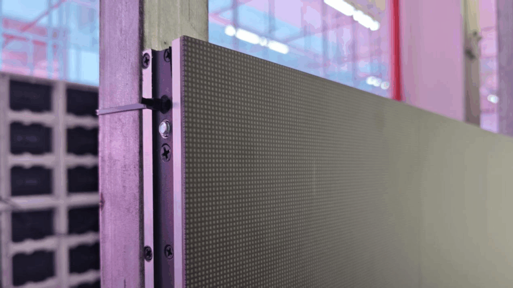
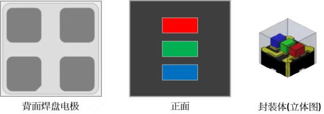
Chip-on-Board (COB) is an advanced LED packaging method where multiple LED chips are bonded directly onto a substrate (typically a PCB) and then encapsulated with a protective phosphor layer. Unlike traditional Surface-Mounted Device (SMD) packaging, COB eliminates the need for individual LED housings, resulting in a more compact and robust design.
-
Key Advantages of COB
(1) Enhanced Durability and Reliability
Since the LED chips are fully encapsulated, COB displays are highly resistant to moisture, dust, and physical impact, making them ideal for harsh environments.
The absence of wire bonding reduces the risk of mechanical failure, improving long-term performance.
(2) Superior Thermal Management
The direct attachment of LED chips to the substrate enhances heat dissipation, reducing thermal stress and extending LED lifespan.
This makes COB particularly suitable for high-brightness applications where heat generation is a concern.
(3) Fine-Pitch Capability
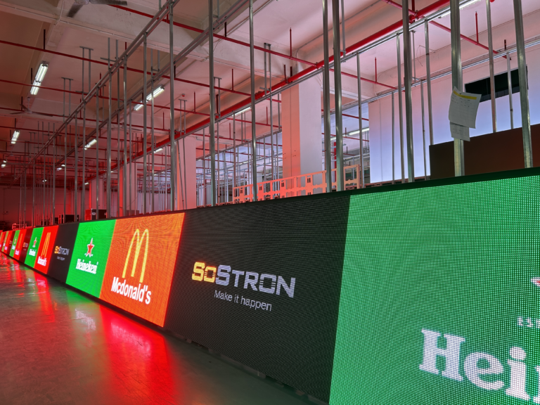
COB enables ultra-fine pixel pitches (P0.4–P1.2), supporting high-resolution displays for control rooms, broadcast studios, and virtual production.
The seamless surface eliminates gaps between pixels, improving image uniformity.
(4) Better Optical Performance
Wider viewing angles (up to 170°) due to the absence of reflectors.
Higher contrast ratios because of reduced light diffusion.
-
Challenges of COB Technology
Despite its benefits, COB faces several limitations:
Higher manufacturing costs due to complex assembly processes.
Difficult repair procedures damaged pixels often require entire module replacement.
Limited scalability for ultra-micro displays (below P0.4), where MIP holds an advantage.
MIP Technology: Revolutionizing Micro-LED Displays
-
What is MIP?
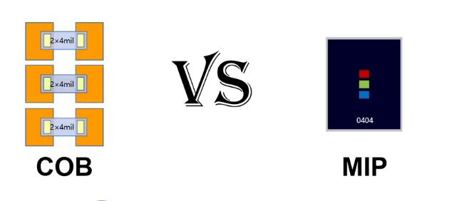
Micro Integrated Packaging (MIP) is an innovative packaging technique designed specifically for Micro-LED applications. Unlike COB, which mounts bare LED chips, MIP integrates multiple Micro-LED chips into a single package, optimizing electrical connections and light conversion efficiency.
-
Key Advantages of MIP
(1) Ideal for Micro-LED Mass Production
MIP enables high-yield mass transfer of Micro-LED chips, a critical requirement for commercializing Micro-LED TVs, AR/VR devices, and wearables.
The integrated packaging reduces defect rates during assembly.
(2) Ultra-Fine Pixel Pitch (<P0.4)
MIP supports sub-micron pixel pitches, making it the preferred choice for next-gen 8K+ displays.
Enables seamless video walls with no visible gaps.
(3) Higher Brightness and Efficiency
Improved light extraction efficiency due to optimized packaging.
Lower power consumption compared to traditional Mini-LED backlighting.
(4) Design Flexibility
Supports flexible and curved displays, opening new possibilities for automotive displays, foldable screens, and transparent LED panels.
-
Challenges of MIP Technology
While promising, MIP still faces hurdles:
High production costs due to precision alignment requirements.
Limited industry standardization, leading to compatibility issues.
Competition from mature technologies like COB and SMD.
Comparison of COB vs. MIP Technologies
- Basic Characteristics
- Packaging Process:
COB: Direct chip mounting + full encapsulation
MIP: Pre-packaged micro-LED units + secondary integration
- Applicable Pixel Pitch:
COB: P0.4–P1.2mm (mainstream fine-pitch)
MIP: <P0.4mm (ultra-fine pitch)
- Performance Comparison
- Reliability:
COB: Fully encapsulated, excellent moisture/dust resistance
MIP: Modular structure, reliability improves with process maturity
- Maintainability:
COB: Requires full module replacement
MIP: Supports individual unit replacement
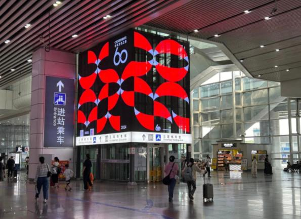
III. Applications & Cost Efficiency
- Applications:
COB: Professional displays (control rooms, studios, etc.)
MIP: Consumer electronics (Micro-LED TVs, AR/VR)
- Cost:
COB: Higher material cost, mid-to-high price range
MIP: High initial equipment investment but faster cost reduction at scale
Future Trends and Industry Outlook
- COB’s Continued Dominance in Professional Displays
COB will remain the leading choice for high-end indoor displays where durability and reliability are critical.
Expected improvements in cost efficiency will expand its adoption in corporate, education, and healthcare sectors.
- MIP as the Future of Micro-LED Commercialization
As mass transfer technologies mature, MIP will drive cost reductions in Micro-LED production.
Major growth expected in consumer electronics (TVs, smartphones, tablets) and emerging markets (smart glasses, automotive displays).
- Hybrid Solutions: Combining COB and MIP Strengths
Some manufacturers are exploring hybrid approaches, using COB for larger LEDs and MIP for Micro-LEDs, optimizing both cost and performance.
- Emerging Applications
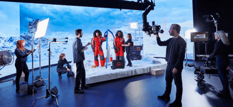
Virtual Production & XR Studios – Both COB and MIP enable high-resolution LED volumes for immersive filming.
Transparent & Flexible Displays – MIP’s design flexibility supports innovative form factors.
Integration with Emerging Technologies
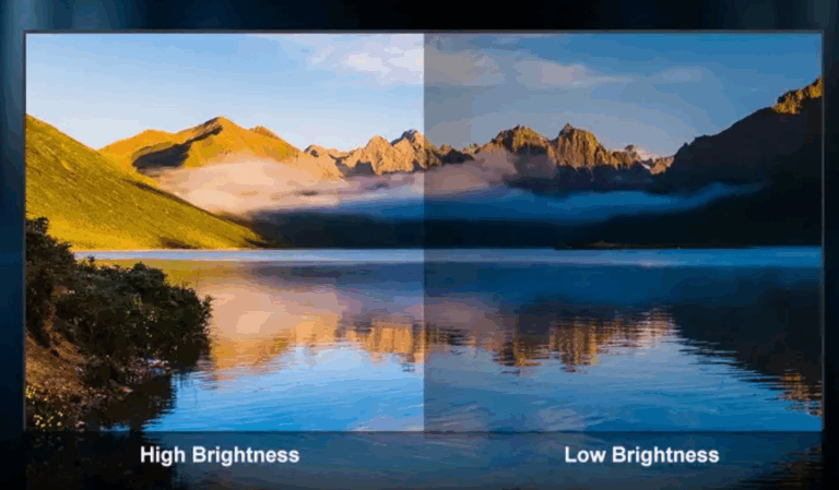
The convergence of COB/MIP with other cutting-edge technologies is creating transformative possibilities. COB displays are being integrated with AI-powered content management systems for dynamic brightness adjustment, reducing energy use by up to 40%. MIP’s precision enables direct integration with quantum dot color conversion layers, achieving 110% NTSC color gamut without additional optical films. Both technologies are proving essential for 5G-enabled smart city applications, where COB provides the durability for outdoor digital signage and MIP enables high-resolution indoor wayfinding. The combination with touch and gesture recognition technologies is creating new interactive possibilities, from large-scale collaborative workspaces to automotive infotainment systems that respond to both touch and mid-air gestures.
Conclusion
The LED display industry is at a pivotal point, with COB and MIP technologies shaping the future of visual solutions. COB excels in reliability and fine-pitch applications, while MIP unlocks the potential of Micro-LEDs for ultra-high-resolution displays.
As manufacturing processes improve and costs decline, both technologies will coexist, each serving distinct market needs. The next decade will likely see further convergence of these technologies, leading to even more advanced and affordable LED display solutions.
By Ivy