The Question Every Buyer Asks
GOB or COB — which one should you actually specify?
The confusion is understandable. Both technologies improve on standard SMD LED packaging, both claim better protection and image quality, and suppliers often use the terms interchangeably in marketing materials. The reality is more precise: GOB and COB solve different problems at different price points, and choosing the wrong one for your application means either overpaying or under-specifying.
Here’s the direct answer: if your project requires pixel pitches below P1.5 and prioritizes image uniformity and long-term reliability, COB is the correct choice in 2026. If you need robust protection for a P1.5–P2.5 outdoor or rental display at a lower upfront cost, GOB delivers strong value. Everything else in this guide explains why.
What Is GOB Technology?
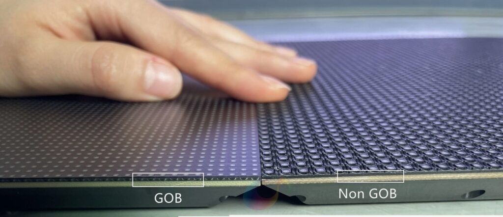
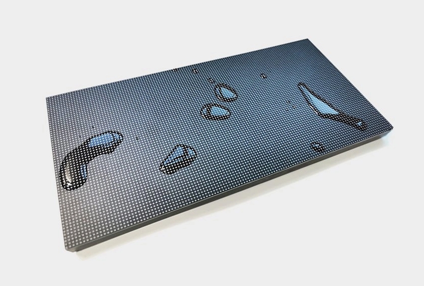
GOB stands for Glue On Board. The process starts with a standard SMD LED display — individual LED beads soldered onto a PCB — and then floods the entire surface with a transparent optical-grade epoxy or silicone resin. Once cured, this glue layer encapsulates the LED beads, solder joints, and PCB surface in a single protective shell.
How GOB Works
The optical glue used in GOB serves three simultaneous functions:
- Mechanical protection — absorbs impact and prevents physical damage to LED beads
- Environmental sealing — blocks moisture, dust, and corrosive gases from reaching solder joints
- Optical enhancement — reduces surface light reflection, improving perceived contrast
GOB is fundamentally a post-process upgrade applied to existing SMD manufacturing lines. This is both its strength (lower cost, compatible with mature SMD supply chains) and its limitation (constrained by the underlying SMD bead size, which limits minimum pixel pitch).
GOB Protection Ratings
| GOB Grade | IP Rating | Impact Resistance | Typical Application |
|---|---|---|---|
| Standard GOB | IP54 | Moderate | Semi-outdoor, covered installations |
| Enhanced GOB | IP65 | Good | Outdoor fixed, rental |
| Premium GOB | IP67 | High | Harsh outdoor, industrial |
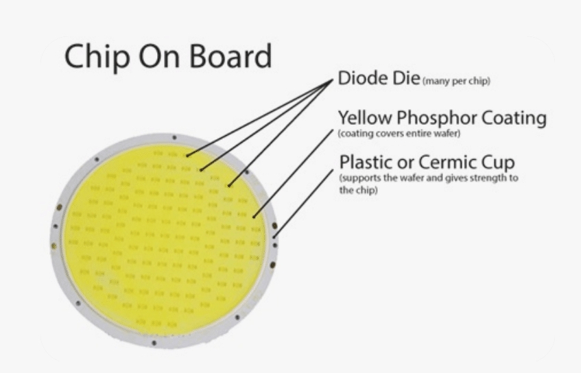
What Is COB Technology?
COB stands for Chip On Board. Instead of packaging LED chips into individual SMD beads first, COB bonds bare LED chips (red, green, blue) directly onto the PCB substrate using conductive adhesive, then wire-bonds them and applies a single phosphor or resin encapsulant over the entire chip array.
Why COB Architecture Is Fundamentally Different
Eliminating the individual bead package has cascading effects on performance:
- Smaller pixel pitch — no bead housing means chips can be placed closer together, enabling P0.4–P0.9 pitches that SMD cannot achieve
- Better thermal path — chips bond directly to PCB copper, reducing junction temperature
- Higher fill factor — more light-emitting area per unit surface, improving brightness uniformity
- Fewer solder joints — each SMD bead requires two solder points; COB eliminates these, reducing failure points by 60–80%
COB is a fundamentally different manufacturing process, not an add-on. This is why COB displays cost more — the production line, equipment, and yield management are all more complex.
7 Differences Between GOB and COB: Full Comparison
| Dimension | GOB | COB | Verdict |
|---|---|---|---|
| Encapsulation method | Optical glue over SMD beads on PCB | Bare chips bonded directly to PCB | Different architectures, not comparable grades |
| Minimum pixel pitch | P1.2 (practical limit) | P0.4 (achievable in 2026) | COB wins for fine-pitch |
| Protection level | IP54–IP67 (glue layer) | IP54–IP65 (encapsulant layer) | Comparable; GOB slightly ahead at high grades |
| Brightness | 800–1,500 nits (indoor) | 1,000–2,000 nits (indoor) | COB higher due to better fill factor |
| Contrast ratio | 3,000:1–8,000:1 | 5,000:1–15,000:1 | COB superior |
| Heat dissipation | Moderate (glue adds thermal resistance) | Better (direct chip-to-PCB path) | COB superior |
| Repairability | Module swap; individual bead replacement possible | Module swap only; chip-level repair not field-serviceable | GOB easier to repair |
| Cost (per m²) | 1,500–4,000 | 3,000–12,000 | GOB lower cost |
| Uniformity | Good | Excellent | COB superior |
| Lifespan | 80,000–100,000 hrs | 80,000–100,000 hrs | Comparable |
| Viewing angle | 120°–140° | 140°–160° | COB slightly wider |
Protection Performance: A Closer Look
Both technologies improve on bare SMD, but the protection mechanisms differ in important ways.
GOB protection comes from the glue layer’s physical barrier. It’s highly effective against:
- Dust ingress (IP6X rated versions)
- Moisture and humidity
- Casual impact (dropped objects, cleaning brushes)
- Corrosive gases in industrial environments
The limitation: if the glue layer cracks under severe impact, the underlying SMD beads are exposed. Glue delamination is also a failure mode in extreme temperature cycling environments.
COB protection comes from the encapsulant bonded directly to the chip surface. Because there are no individual bead housings to crack or detach, COB handles vibration and repeated mechanical stress better. The flat surface is also easier to clean without risk of dislodging components.
For rental displays that are assembled and disassembled repeatedly, COB’s flat, seamless surface is more durable under handling stress than GOB’s glue-coated bead array.
Heat Dissipation: Why It Matters for Longevity
LED junction temperature is the primary driver of lifespan degradation. Every 10°C increase in junction temperature roughly halves LED lifespan.
| Technology | Thermal Path | Typical Junction Temp (full brightness) | Impact on Lifespan |
|---|---|---|---|
| Standard SMD | Chip → bead housing → solder → PCB | 65–80°C | Baseline |
| GOB | Chip → bead housing → solder → PCB → glue (adds resistance) | 70–85°C | Slightly worse than SMD at high brightness |
| COB | Chip → conductive adhesive → PCB copper | 55–70°C | Better than SMD; best longevity |
GOB’s optical glue adds a small amount of thermal resistance to the existing SMD thermal path. At moderate brightness levels this is negligible, but at sustained high brightness (outdoor applications running at 5,000+ nits), the thermal penalty becomes measurable. COB’s direct chip bonding provides the shortest thermal path of any packaging approach.
Cost Analysis: What You’re Actually Paying For
The cost difference between GOB and COB is real and significant, but the reasons are often misunderstood.
GOB cost drivers:
- Base SMD display cost (unchanged)
- Glue material and application process (adds 15–30% to SMD base cost)
- Curing equipment and quality inspection
- No fundamental change to LED chip or PCB design
COB cost drivers:
- Specialized die-bonding equipment (significantly more expensive than SMD pick-and-place)
- Bare chip procurement (different supply chain from packaged SMD beads)
- Higher yield management complexity (defects are harder to detect pre-encapsulation)
- Advanced calibration required for uniformity
| Configuration | GOB (P1.5, indoor) | COB (P1.5, indoor) | COB (P1.2, indoor) | COB (P0.9, indoor) |
|---|---|---|---|---|
| Hardware cost/m² | 1,800–3,500 | 3,500–6,000 | 5,000–9,000 | 8,000–15,000 |
| Installation/m² | 600–1,200 | 800–1,500 | 1,000–2,000 | 1,500–3,000 |
| 5-yr maintenance/m² | 400–800 | 300–600 | 300–600 | 400–800 |
| 5-yr TCO/m² | 2,800–5,500 | 4,600–8,100 | 6,300–11,600 | 9,900–18,800 |
Application Matching: Which Technology for Which Project
Choose COB When:
- Pixel pitch is P1.5 or below — COB is the industry standard at this range in 2026
- The installation is a permanent indoor environment (control room, boardroom, retail flagship)
- Image uniformity is critical (broadcast, medical imaging, color-accurate retail)
- The display will run 16–24 hours daily — COB’s thermal advantage compounds over time
- Budget allows for higher upfront investment with lower long-term maintenance
Choose GOB When:
- Pixel pitch is P1.5–P3.9 and budget is a primary constraint
- The application is outdoor fixed installation requiring IP65+ protection
- The display is rental/touring and needs robust handling durability at moderate pitch
- Existing SMD infrastructure is being upgraded rather than replaced
- Field repairability is a priority (individual bead replacement is possible with GOB)
Application Decision Matrix
| Application | Recommended Technology | Pixel Pitch | Rationale |
|---|---|---|---|
| Indoor fine-pitch video wall | COB | P0.9–P1.5 | Uniformity and brightness critical |
| Corporate boardroom | COB | P1.2–P1.9 | Close viewing distance, image quality priority |
| Outdoor advertising (fixed) | GOB | P2.5–P3.9 | IP protection, cost efficiency |
| Rental/event display | GOB or COB | P1.5–P2.9 | GOB for budget; COB for premium events |
| Control room / NOC | COB | P0.9–P1.5 | 24/7 operation, uniformity, longevity |
| Retail window display | COB | P1.2–P1.9 | High ambient light, color accuracy |
| Stage backdrop | GOB | P2.5–P3.9 | Viewing distance, cost, handling durability |
| Semi-outdoor (covered) | GOB | P1.9–P3.9 | IP54 sufficient, cost advantage |
2026 Industry Trends: Where GOB and COB Are Heading
The market has moved decisively toward COB for fine-pitch applications. In 2026, the majority of new indoor fine-pitch installations at P1.5 and below specify COB as the default. Key developments:
- MIP (Micro LED in Package) is emerging as a third option between COB and true Micro LED, offering COB-level performance with improved repairability. Expect MIP to gain share in the P0.9–P1.5 range through 2027.
- GOB is consolidating around outdoor and rental — its cost advantage is most defensible in P2.0+ applications where COB’s fine-pitch benefits don’t apply.
- Yield improvements in COB manufacturing have reduced the cost premium versus GOB at P1.5 by approximately 20–25% since 2023, accelerating COB adoption.
- Flat-surface COB has become the standard for rental applications, replacing GOB in premium touring productions where image quality justifies the cost.
Conclusion
GOB and COB are not competing grades of the same technology — they are different manufacturing architectures that excel in different contexts. GOB is a cost-effective protection upgrade for SMD displays in the P1.5–P3.9 range. COB is the correct specification for fine-pitch indoor applications at P1.5 and below, where its superior uniformity, brightness, and thermal performance justify the higher investment.
In 2026, the industry has largely settled this debate for fine-pitch applications: COB is the standard. For outdoor, rental, and budget-constrained projects at larger pitches, GOB remains a strong and practical choice.
SoStron manufactures both technologies across a full pitch range, with in-house calibration systems and module-level serviceability designed for long-term commercial deployments. Our engineering team can help you match the right packaging technology to your specific application, budget, and operational requirements.