Quick Answer: COB delivers the best visual uniformity and durability for fine-pitch indoor applications (P0.4–P1.5); SMD remains the cost-efficient, field-serviceable workhorse for outdoor DOOH and rental staging (P1.2–P10+); Mini LED commands premium positioning for broadcast-grade HDR and XR virtual production. The table below is your starting point.
| Feature | SMD | COB | Mini LED |
| Best Pixel Pitch | P1.2–P10+ | P0.4–P1.5 | P0.7–P1.5 |
| Peak Brightness | 2,000–5,000 nits | 800–1,500 nits | 1,000–2,000 nits |
| Repairability | On-site, single LED | Module-level only | Module-level only |
| 5-Year TCO | Medium | Low–Medium | High |
| Core Strength | Versatility & cost | Durability & image quality | Contrast & HDR |
Every quarter, our team evaluates dozens of B2B LED display projects—from 800 sqm DOOH networks in Southeast Asia to mission-critical command centers in the Middle East. The single most common mistake we see buyers make? Selecting packaging technology based on unit price alone.
A system integrator recently forwarded us a competitor’s quote: COB at P1.2, priced 18% higher than an equivalent SMD spec. The client almost declined. What the quote didn’t show was the 5-year maintenance projection—once we modeled the SMD module replacement frequency against COB’s ~0.5% annual failure rate, COB’s total cost of ownership came in 31% lower. That procurement decision was worth $140,000 over the contract period.
This guide exists to prevent that miscalculation. Based on our direct experience across hundreds of commercial installations—and drawing on Omdia’s Q1 2026 LED Video Displays Market Tracker, which confirmed fine-pitch displays now represent 55.4% of total LED display revenue—we break down COB, SMD, and Mini LED packaging across every dimension that actually matters to a B2B buyer.
What Is LED Display Packaging Technology—And Why It Directly Determines Your Project’s ROI
Before you compare specifications, you need to understand what LED packaging actually controls. Think of packaging as the architectural decision that happens before a single panel ships: it governs how the LED chip is mounted, protected, and electrically connected to the PCB. Get this decision wrong, and no amount of downstream optimization—calibration, thermal management, content processing—will fix the structural limitations baked into the hardware.
Packaging technology directly determines four commercially critical variables:
-
Pixel pitch floor—how fine a resolution is physically achievable.
-
Thermal path—how efficiently heat travels from chip to PCB, which directly governs lifespan.
-
Mechanical resilience—how the display survives shipping, installation, and daily operation.
-
Serviceability model—whether a failed pixel costs you $3 or $300 to fix, and whether it can be done on-site or requires factory return.
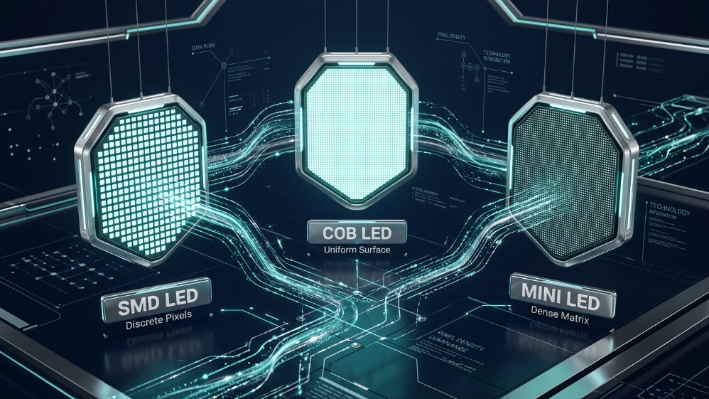
The LED packaging roadmap has evolved through four generations: DIP (through-hole, largely obsolete for commercial displays), SMD (the current mainstream), COB (the dominant fine-pitch technology), and now Mini LED/MIP (emerging for specialized high-performance segments). Each generation solved a specific problem introduced by the previous one. Understanding that lineage tells you exactly why each technology still occupies its market position today.
SMD LED Display Packaging: The Industry’s Proven Foundation
SMD—Surface-Mounted Device—has been the backbone of the commercial LED display industry for over a decade. There’s a reason it still dominates: it is a spectacularly well-optimized solution for the problems it was designed to solve.
How SMD Technology Works
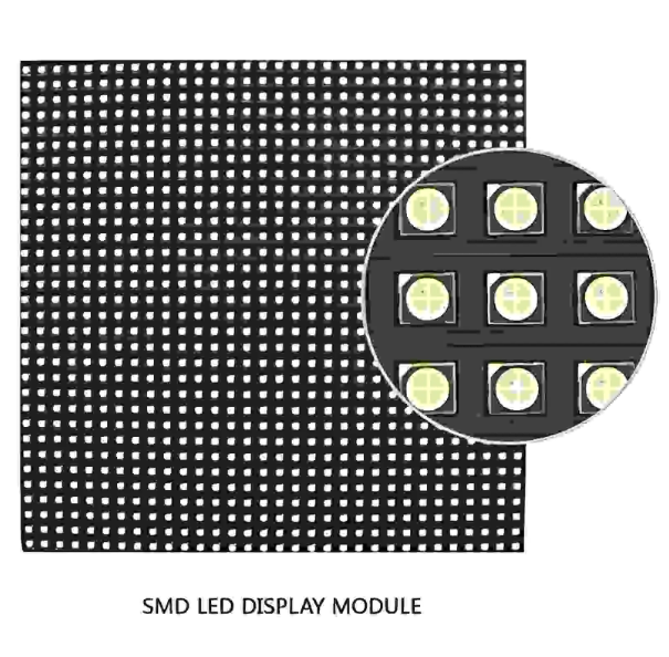
In SMD packaging, red, green, and blue LED chips are individually encapsulated into small plastic housings—the components you can physically see as distinct “beads” on a display panel. These pre-packaged components are then placed onto the PCB surface via automated SMT (Surface-Mount Technology) pick-and-place machines and permanently bonded through reflow soldering.
This multi-step process—lamp packaging → SMT placement → reflow soldering → module assembly—is mature, extensively automated, and supported by a deep global supply chain. That supply chain maturity is not a minor footnote: it translates directly into competitive pricing, fast lead times, and—critically for large-scale deployments—a global ecosystem of replacement components.
Where SMD Wins for B2B Buyers
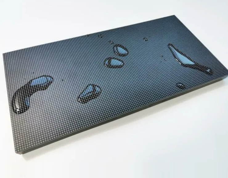
For outdoor DOOH operators, SMD’s brightness ceiling is decisive. Outdoor SMD configurations routinely deliver 2,000–5,000 nits, with specialized configurations exceeding 7,000 nits—necessary to overcome direct sunlight in high-traffic urban environments. IP65-rated weather-sealing has been field-tested and refined over years of real-world deployments in environments ranging from Singaporean humidity to Saudi desert heat.
For event and rental companies, the field repairability advantage is non-negotiable. When a display panel fails mid-event at 11pm, the ability for a technician to swap a single SMD lamp bead on-site—rather than returning a module to a factory—is the difference between a minor inconvenience and a client relationship ending. SMD’s modular, replaceable component architecture was built for exactly this operational reality.
For budget-sensitive standard installations, SMD’s mature manufacturing process means production yields are high and costs are predictable. At pixel pitches of P2.0 and above, SMD remains the rational default.
Where SMD Reaches Its Physical Limits
The same encapsulation structure that makes SMD reliable and repairable also imposes a hard ceiling on what’s physically achievable. Each SMD component has minimum dimensional constraints—the plastic housing, the solder points, the spacing required between individual beads. Below approximately P1.2, these constraints become a fundamental barrier. You cannot simply “make SMD smaller” without compromising yield rates and structural integrity.
Additionally, because SMD creates a point light source array—discrete light-emitting points with physical gaps between them—viewers at close range perceive visible pixel separation. At a 2-meter viewing distance on a P2.5 SMD wall, this isn’t an issue. In a corporate boardroom where executives sit 1.5 meters from a P1.5 display, it becomes a quality problem that no content calibration can solve.
COB LED Display Packaging: The Architecture That Changes the Image Quality Equation
COB—Chip-on-Board—takes a fundamentally different structural approach. Instead of pre-packaging individual LED chips into discrete components, COB bonds multiple bare RGB chips directly onto the PCB substrate. The entire array is then encapsulated under a continuous, seamless layer of protective epoxy resin.
The result is not just an incremental improvement over SMD. It’s a different category of display surface.
Standard Wire-Bond COB vs. Flip-Chip COB: A Distinction Most Buyers Miss
This distinction is where most comparison guides—and frankly, most sales conversations—fail B2B buyers. There are two materially different generations of COB technology currently being shipped, and they perform very differently.
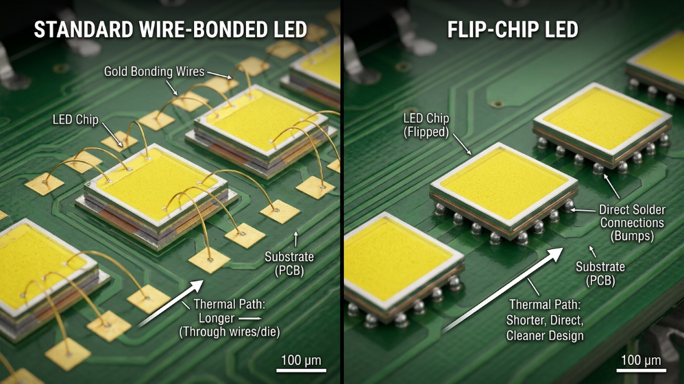
Standard (Wire-Bond) COB uses thin gold or copper bonding wires to connect each LED chip to the PCB circuit. It’s more integrated than SMD, but those wires introduce micro-mechanical stress points and limit how short the thermal path can be.
Flip-Chip COB eliminates bonding wires entirely. The LED chip is literally flipped and connected face-down, directly to the PCB’s copper layer. This architectural change is significant:
| Feature | Wire-Bond COB | Flip-Chip COB |
| Bonding Wire Solder Points | Present | Eliminated (↓40%) |
| Failure Rate vs. SMD | ~30–40% lower | ~50% lower |
| Thermal Path Length | Short | Ultra-short (direct copper contact) |
| Energy Consumption | Moderate reduction vs. SMD | Up to 40% lower vs. SMD |
| Pixel Pitch Floor | P0.9 (stable) | P0.4 (achievable) |
| ESD Resistance | High | Very High |
| Market Availability | Mainstream | Premium; rapidly scaling |
When a supplier quotes you “COB technology,” always ask which generation. The answer affects every performance metric you’re evaluating.
The Manufacturing Process Behind COB’s Visual Advantage
COB’s encapsulation process converts what would be a field of individual point light sources into a continuous surface light source. The epoxy resin layer creates optical integration across the entire module—light from adjacent chips blends before it exits the surface.
For a B2B buyer, this translates into three commercially meaningful outcomes:
-
Zero visible pixel structure at close viewing distances—the “screen door” effect that plagues fine-pitch SMD disappears entirely.
-
Wider effective viewing angles with minimal color shift, because you’re not looking at individual point emitters at oblique angles.
-
Significantly reduced eye fatigue during extended viewing sessions—a specification that matters in control rooms and corporate environments where operators spend 8+ hours per day in front of displays.
These aren’t aesthetic preferences. In a 24/7 traffic management center or a financial trading floor, display-induced eye fatigue is a workplace health and productivity variable with measurable business cost.
COB’s Durability Advantage: The Numbers Behind the Claim
The monolithic epoxy encapsulation that gives COB its optical properties also functions as a structural armor. Unlike SMD, where each individual lamp bead is a discrete component exposed at the surface, COB’s continuous resin layer absorbs mechanical impact across the entire module surface. Independent pressure testing on leading flip-chip COB modules has demonstrated resistance exceeding 100kg/cm²—meaning a display that survives the logistics chain from Shenzhen to a São Paulo installation site without dead pixels is a realistic expectation, not a marketing promise.
ESD resistance follows the same logic. In SMD displays, electrostatic discharge events can destroy individual lamp beads selectively—you end up with scattered dark pixels that are individually cheap to replace but cumulatively expensive to manage across a large installation. COB’s encapsulated structure distributes and dissipates electrostatic energy across the module rather than concentrating it at vulnerable chip-wire junctions.
In practice, this translates to an annual pixel failure rate of approximately 0.5% for COB versus 1.5–3% for SMD in comparable indoor fine-pitch deployments. Applied across a 200-panel control room installation running 16 hours per day, that difference isn’t theoretical—it’s a maintenance schedule, a labor budget, and a downtime risk model.
Mini LED Display Packaging: Precision Optical Engineering for Demanding Environments
Mini LED occupies a distinct and frequently misunderstood position in the B2B display landscape. The confusion stems from terminology: “Mini LED” describes a chip size category (100–300 microns), not a single packaging method. In the consumer market, Mini LED almost always refers to backlight technology in LCD panels. In direct-view commercial displays, Mini LED chips are integrated into advanced packaging architectures—most commonly COB-based—to push pixel density and optical performance beyond what conventional SMD allows.
For B2B buyers, the commercially relevant question isn’t “Mini LED vs. COB” as competing categories. It’s: does your project require the specific optical performance that Mini LED chip architecture enables, and can your budget and operational model support its total cost structure?
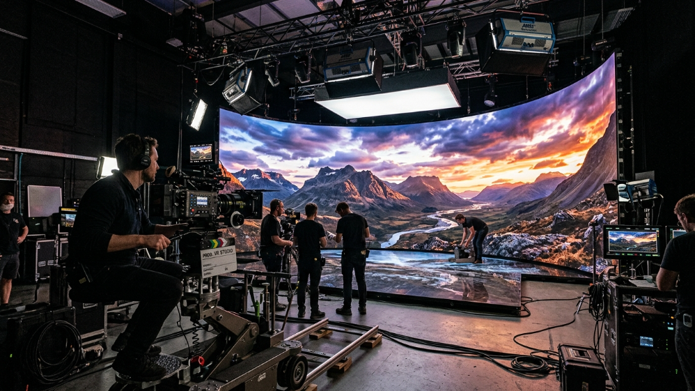
The answer is yes for a narrow but important set of applications. Broadcast studios running simultaneous camera capture require displays with virtually zero moiré interference and near-zero black-level luminance—Mini LED’s local dimming zone architecture, capable of million-to-one contrast ratios, addresses this directly. XR virtual production stages where LED volumes must match camera sensor dynamic range in real time have no viable alternative at current technology maturity levels. High-end medical imaging environments, where a misrepresented dark tone could influence a clinical decision, justify the premium.
For everything outside these specialized applications, Mini LED’s complexity—optical film stack requirements (diffuser film, prism film, reflective polarizer), driver IC zone-mapping algorithms, and the resulting calibration overhead—introduces cost and maintenance variables that most B2B installations don’t need and can’t efficiently manage.
The 6-Dimension Full Comparison: COB vs SMD vs Mini LED
This table is designed to function as a procurement reference document. Share it with your technical team and procurement committee—the dimensions map directly to the evaluation criteria in most enterprise RFQ frameworks.
| Evaluation Dimension | SMD | COB (Flip-Chip) | Mini LED |
| Unit Cost (per sqm, P1.5) | Low (1.0×) | Medium (1.15–1.25×) | High (1.6–2.2×) |
| Pixel Pitch Range | P1.2–P10+ | P0.4–P2.0 | P0.7–P1.5 |
| Peak Brightness | 2,000–7,000 nits | 800–1,500 nits | 1,000–2,500 nits |
| Contrast Ratio | 3,000:1–5,000:1 | 5,000:1–10,000:1 | Up to 1,000,000:1 |
| Annual Failure Rate | 1.5–3% | ~0.5% | ~0.8–1.2% |
| Repairability | On-site single LED | Module replacement | Module replacement |
| ESD/Impact Resistance | Moderate | Very High | High |
| Viewing Angle Consistency | Good | Excellent | Excellent |
| Eye Fatigue | Moderate | Low | Low |
| 5-Year Maintenance Index | 1.0× | 0.3–0.5× | 0.7–1.0× |
| Outdoor Viability | ✅ Primary choice | ⚠️ Limited | ⚠️ Emerging only |
| Future Roadmap | Approaching limits | Strong (Micro LED pathway) | Strong (Native architecture) |
| Ideal B2B Application | DOOH, Rental, Retail | Control rooms, Boardrooms | Broadcast, XR, Cinema |
One number in that table deserves direct commentary: the 5-year maintenance cost index. Based on documented commercial deployment data from high-traffic retail environments, COB installations have demonstrated maintenance cost reductions of up to 73% versus SMD equivalents over a five-year operational period. The mechanism is straightforward—fewer failure events, combined with COB’s inherent anti-collision structure, reduces both parts consumption and technician dispatch frequency. For any installation with a service contract or internal AV maintenance team, this figure belongs in your financial model before sign-off.
The Packaging Decision Framework: A Practical Guide for B2B Buyers
Specifications only become useful when mapped to operational context. Here is how the three packaging technologies align to the B2B buyer profiles most active in the current market:
-
System Integrators (Fixed Installation): For any project specifying P1.5 or below in an indoor environment—control rooms, data visualization centers, command centers, executive briefing rooms—flip-chip COB is the technically sound default. The MTBF advantage and surface light source quality are unambiguous at this pitch range. For outdoor fixed installations above P2.0, SMD with IP65 certification remains the rational specification.
-
DOOH Network Operators: Outdoor DOOH economics are driven by uptime, brightness, and cost-per-sqm at scale. SMD wins on all three in standard configurations. The emerging exception: premium city-center digital OOH installations at P2.0 or below, where image quality is a brand differentiator—COB is beginning to penetrate this segment as fine-pitch outdoor COB modules scale in availability.
-
Event and Rental Companies: Field repairability is not a preference—it’s a business continuity requirement. SMD’s ability to swap a single failed lamp bead at a venue, without tools beyond a soldering iron and steady hands, is irreplaceable for live event operations. Rental companies evaluating COB should factor dedicated spare module inventory (typically 5–8% of total panel count) into their capital planning.
-
Broadcast and XR Production: Mini LED or flip-chip COB with HDR-optimized processing. The contrast ratio and black-level uniformity requirements of camera-facing LED volumes eliminate SMD as a primary option for this segment.
5 Questions B2B Buyers Ask—Answered Directly
Q1: Is COB LED display worth the higher upfront cost compared to SMD?
At pixel pitches of P1.5 and below for indoor applications: yes, consistently. The 10–20% unit cost premium is typically recovered within 18–30 months through reduced maintenance expenditure and lower technician dispatch costs. At P1.2 specifically, COB pricing has already reached parity with—and in some configurations fallen below—equivalent SMD products as manufacturing volumes have scaled. The premium argument is weakening at fine pitches even before TCO enters the conversation.
Q2: Can COB LED displays be repaired on-site like SMD?
Not in the conventional sense. COB’s monolithic encapsulation means individual chip replacement is not field-viable—the heat required to rework a single pixel risks visible thermal distortion across the surrounding resin surface. The operational response to COB failure is module-level replacement. This makes pre-positioning spare module inventory essential for large installations. Budget approximately 3–5% of total panel count as on-site spares for mission-critical deployments.
Q3: What exactly is “flip-chip COB” and should I specify it in my RFQ?
Flip-chip COB eliminates bonding wires by inverting the LED chip and connecting it directly to the PCB copper layer. The practical outcome: solder point count drops by approximately 40%, failure rates decrease by roughly 50% versus standard wire-bond COB, and thermal dissipation improves measurably—translating to lower operating temperatures and extended MTBF. Yes, you should specify it explicitly in RFQs for any fine-pitch indoor installation. If a supplier cannot confirm which COB generation they’re quoting, treat that as a qualification signal.
Q4: Is Mini LED the same technology as what’s in consumer Mini LED TVs?
No—and this confusion costs B2B buyers time and credibility in procurement discussions. Consumer Mini LED TVs use Mini LED chips as a backlight behind an LCD panel to improve local dimming. Direct-view commercial LED displays use Mini LED chips as the primary light source, visible directly to the viewer. The applications, performance profiles, and cost structures are entirely different. When evaluating commercial display proposals, always confirm whether “Mini LED” refers to a direct-view configuration or a backlight-enhanced LCD hybrid.
Q5: Which packaging technology is best future-proofed against the Micro LED transition?
COB—specifically flip-chip COB—has the strongest structural alignment with Micro LED’s technical requirements. Both architectures rely on direct chip-to-substrate bonding, common cathode drive compatibility, and integrated encapsulation. Manufacturers already scaling flip-chip COB production are effectively building the manufacturing infrastructure that Micro LED mass production will require. SMD’s physical limits are unlikely to extend meaningfully into sub-P0.9 territory. For buyers making 7–10 year infrastructure decisions, COB’s position on the Micro LED development pathway is a legitimate procurement consideration, not a vendor talking point.
Expert Verdict

Three technologies, three distinct operating envelopes. SMD remains the most rational choice for any project where outdoor brightness, field serviceability, or budget efficiency outweighs image quality at close range—which still covers the majority of global LED display square meters deployed annually. COB has crossed the inflection point: at P1.2 and below, the TCO mathematics now favor it even before you account for visual quality superiority, and flip-chip COB is the specification worth demanding. Mini LED belongs in your shortlist only when the application genuinely requires broadcast-grade HDR performance—and when your operational team is equipped to manage its calibration and maintenance complexity.
The buyers who get this decision right aren’t necessarily the ones with the largest budgets. They’re the ones who separate the capital line item from the operational cost model—and who ask their suppliers the seven questions that confirm whether a specification sheet reflects engineering reality or sales positioning.
References:
Omdia – LED Video Displays Market Tracker
IEEE Xplore – Research on Flip-Chip COB & Mini LED Reliability